The search for the Holy Grail in Analog Design Automation

Introduction:
The optimization of analog circuit sizing has long been recognized as a challenging task within the field. This difficulty has given rise to two distinct approaches to design optimization:
1. Knowledge-based optimization
2. Simulation-based optimization.
In the first approach, referred to as knowledge-based optimization, tools like OASYS and ASTRX/OBLX have been developed. These tools operate on the basis of pre-defined rules and expert knowledge, guiding the optimization process. On the other hand, simulation-based optimization, as exemplified by ANACONDA, relies on simulating the circuit's behavior under various conditions to determine the optimal sizing.
Despite the efforts made by both schools of thought, neither has been successful in creating a widely accepted commercial design automation tool that fully satisfies the expectations of industrial design experts. These expectations include aspects such as design productivity, full traceability, easy debugging, design reuse, quality assurance, minimum cost, and comprehensive design documentation.
Therefore, the question remains: Is analog circuit sizing optimization an NP-Complete or NP-Hard problem ?
Our intention is to delve into this subject matter, carefully dissecting the mathematical principles that underpin this claim, while also striving to construct a fresh computational model capable of effortlessly transforming this problem into a P-type one.
P, NP, NP-Complete and NP-Hard problems:
In computational complexity theory, P, NP, NP-complete, and NP-hard are classes of decision problems.
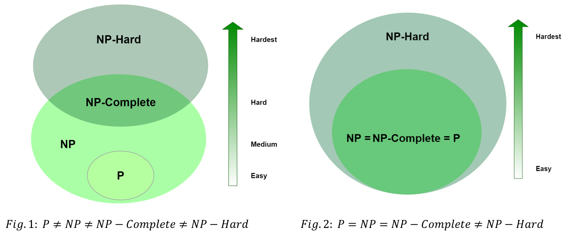
Figure 1: Relations between algorithm complexities.
P (Polynomial Time): P is the class of decision problems that can be solved by a deterministic Turing machine in polynomial time. This means that the solution can be found efficiently with a time complexity of O(n^k), where n is the size of the input and k is a fixed constant.
NP (Nondeterministic Polynomial Time): NP is the class of decision problems that can be verified by a nondeterministic Turing machine in polynomial time. This means that given a potential solution, it can be verified efficiently with a time complexity of O(n^k). However, finding the solution itself may be computationally expensive.
NP-complete: NP-complete problems are a subset of NP problems. A decision problem is NP-complete if every problem in NP can be reduced to it in polynomial time. In other words, if a polynomial-time algorithm exists for one NP-complete problem, then it would imply the existence of polynomial-time solutions for all NP problems. This makes NP-complete problems some of the most challenging and important problems in computer science.
NP-hard: NP-hard problems are a broader class that includes both NP and NP-complete problems. NP-hard problems are at least as hard as the hardest problems in NP. They may or may not be in NP themselves. Essentially, NP-hardness implies that a problem is as difficult as the most difficult problems in NP but does not necessarily mean it is solvable within polynomial time.
Is P=NP Statement Valid?
A question that’s fascinated many computer scientists is whether or not all algorithms in NP belong to P.
For our definitions, we assumed that P≠NP, however, P=NP may be possible. If it were so, aside from NP or NP-Complete or problems being solvable in polynomial time, certain algorithms in NP-Hard would also dramatically simplify. For example, if their verifier is NP or NP-Complete, then it follows that they must also be solvable in polynomial time, moving them into P = NP = NP-Compete as well.
We can conclude that means a radical change in computer science and even in the real-world scenarios. Currently, some security algorithms have the basis of being a requirement of too long calculation time. Many encryption schemes and algorithms in cryptography are based on the number factorization which the best-known algorithm with exponential complexity. If we find a polynomial-time algorithm, these algorithms become vulnerable to attacks.
How did Analog Circuit Optimization start?
Since the 80's, analog circuit optimization was assumed to be NP due to its complex nature. Following the definitions of NP mentioned above, NP problems can be easily verified but are hard to solve. Consequently, it was decided to use an optimization engine to generate candidate solutions and verify each candidate by a performance evaluator such as SPICE simulators. This point of view led to the emergence of simulation-based optimization tools such as ASF, ANACONDA and MAELSTROM as depicted in Figure 2.
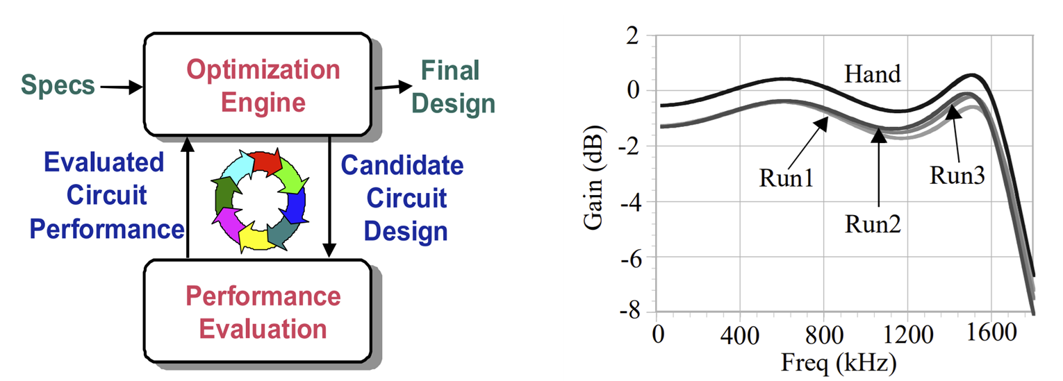
Figure 2: (a) Simulation-based optimization flow, (b) Observation made in [31]
A general and honest observation has been outlined in [31]: despite the huge computational effort used in this work to optimize the Equalizer, the optimization engine was not capable of reaching the precision of hand analysis.
This observation is very fundamental to our analysis and the real questions become:
- Why analog designers can reach a precision that may not be achieved using high computational effort ?
- Why simulation-based optimization failed to meet hand analysis despite the existence of a SPICE simulator in the loop ?
A Deeper Look into SPICE Computational Model:
In order to determine how efficient is the computational model implemented in SPICE simulator, we analyzed graphically the nonlinear DC analysis since it is the only backbone algorithm in SPICE engine. Other analyses such as AC and TRANSIENT are simply variants of the nonlinear DC analysis:
- The AC analysis is a linearization of the circuit around the DC operating point.
- The TRANSIENT analysis is a nonlinear DC analysis with initial conditions varying with time for each timestep.
To measure the complexity of the nonlinear DC analysis implementing the Newton-Raphson algorithm, we modeled the DC analysis as a cyclic graph as illustrated below:
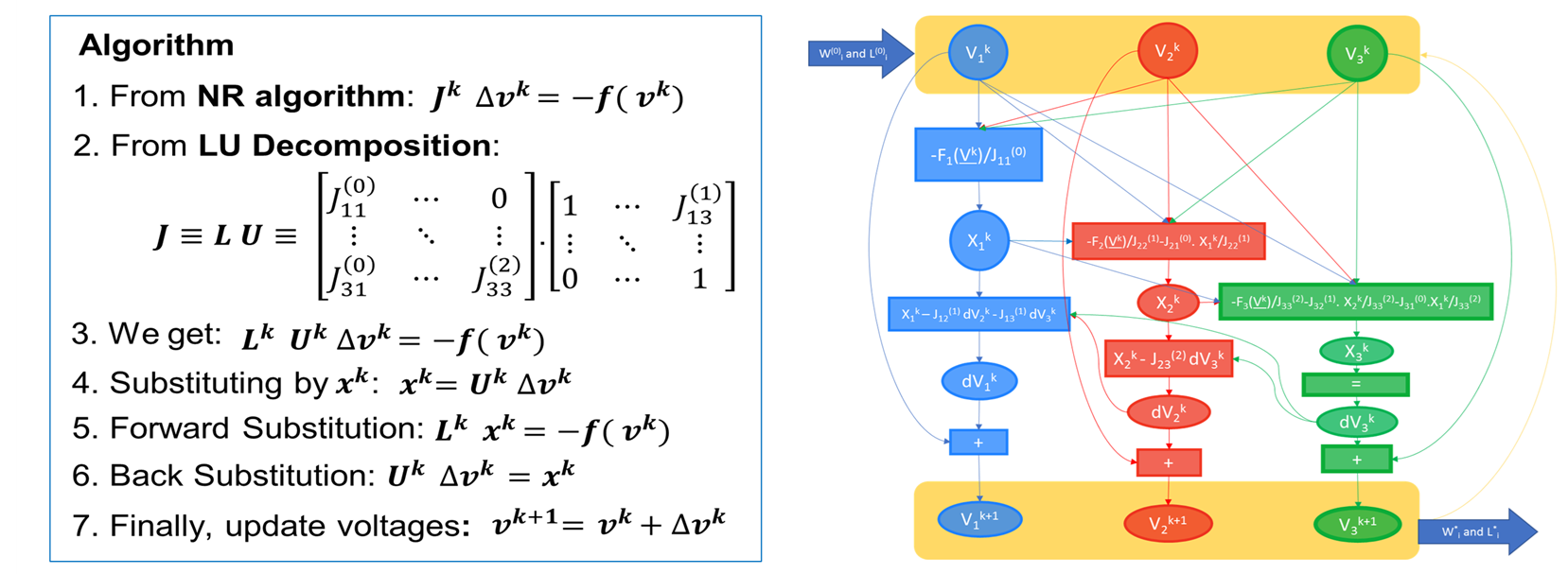
Figure 3: Graph modeling of the nonlinear DC analysis implemented in SPICE.
A deeper look into the graph on the right side reveals how complex is the computation model in SPICE. Loops exist on the level of each vertical branch. Forward and backward values propagation occur from one branch to the next one increasing the dependency between branches. These propagations exist due to the presence of diagonal and nondiagonal Jacobian elements. All these computations occur at each iteration of the nonlinear DC simulation. We conclude that the computational model of SPICE inherently requires lots of computations and suffers from convergence issues due to the presence of Jacobian elements in each forward and backward propagation. Over the years, lots of research efforts led to the reduction of the complexity of the DC analysis to O(n^1.2) = α. n^1.2 where n is the number of node voltages to compute.
To summarize this section, the computational model of SPICE:
- Has a Matrix-based formulation.
- Implements simultaneous nonlinear equations resolution.
- Each iteration requires a large number of computations.
- Jacobian computation becomes a major difficulty.
The next question that arises is the following: Analog designers do not explicitly compute the Jacobian matrix during hand analysis, so how they do it?
Computational Model used by an experienced analog designer
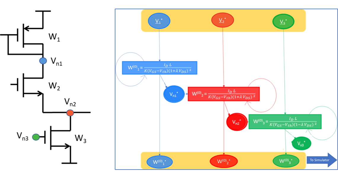
Figure 4: Analog designer manual structured analysis of a typical analog circuit.
To compute the size W1 of the upper transistor in the schematic, the design would propose values for the biasing current, MOS Length and the node voltage Vn1, then he will compute W1 using a simple MOS model. Next, the designer will propagate Vn1 to the next transistor, proposes a vnode voltage Vn2 and then computes W2 assuming same current and Length, and so on.
We conclude that during hand analysis, the model of computation followed by the analog designer is much simpler than the SPICE one since:
- Structured Resolution since each node voltage is computed in sequence.
- No matrix-based formulation.
- Each iteration requires only one computation to determine the size
- Jacobian computation disappeared
Here, the big question that arises is the following: Can we combine the simplicity of the structured resolution approach used during hand analysis with the precision of SPICE simulation to design, explore, optimize and migrate analog circuits ?
Structured Resolution Approach for Analog Design Automation
It is possible to build an analog synthesis system that mimics analog designer behavior during hand analysis but does the same job at SPICE precision. This can be quite easily achieved by replacing MOS level 1 models with standardized API interface for Process Design Kits that are compatible with all device types and all foundries PDKs. The resulting approach is illustrated in Figure 5, where sizing and biasing functions F interface with PDK files to compute the sizes and biases of each transistor sequentially.
Doing so, an efficient Cognitive Computing system has been created by capitalizing on the efficiency of human designers while supported by the accuracy of computer simulation programs.
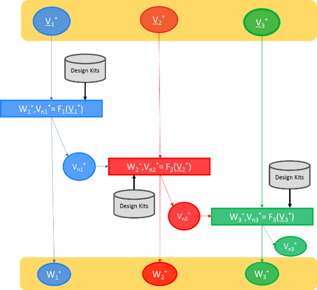
Figure 5: Mimic human cognitive behavior with SPICE accuracy
Here, the next question that arises is: How to build a product to automate analog design and migration?
Digitally-Inspired Analog Circuit Synthesis System
Figure 6 below shows how to build an analog circuit synthesis flow similar to digital high-level synthesis systems that are very mature and in production since decades. The flow for analog will rely on four modules :
1- The schematic scheduler: This module scans the schematic and determines the sequence of transistors to compute in order. Here, it acts like a human designer and implementing cognitive computing strategies.
2- The Function Allocator: This module will assign a sizing and biasing function that shall compute the device biases and geometries based on its connectivity context.
3- Technology Mapper: This module links each transistor to the PDK files based on the requested device variant in order to size and bias the device accurately using standard compact device models or simply accurate DC simulations.
4- Graph Evaluator: In this analog flow, we previously described steps (1)-(3) as directed acyclique graphes that shall be evaluated in step (4) to get sizes and biases.
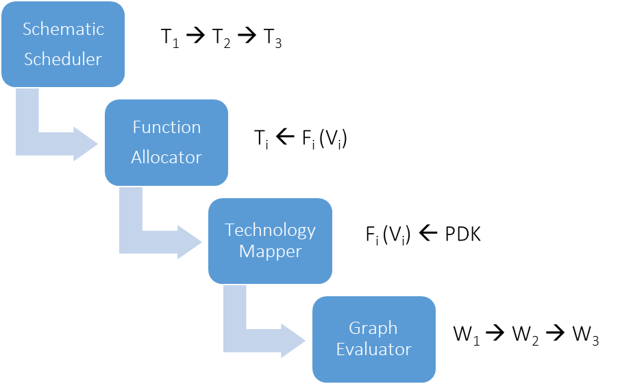
Figure 6: Proposed architecture of the digitally-inspired analog synthesis system
P-type Knowledge Graphs Generated by the synthesis system
To appreciate the proposed methodology, we illustrate in Figure 7 the Miller OTA amplifier to be synthesized:
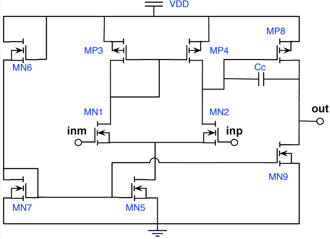
Figure 7: Miller OTA amplifier
Figure 8 shows the corresponding generated bipartite knowledge graph taking as input the designer chosen parameters and the topology of the OTA Miller and computing the size and bias of each device as the output of its allocated function.
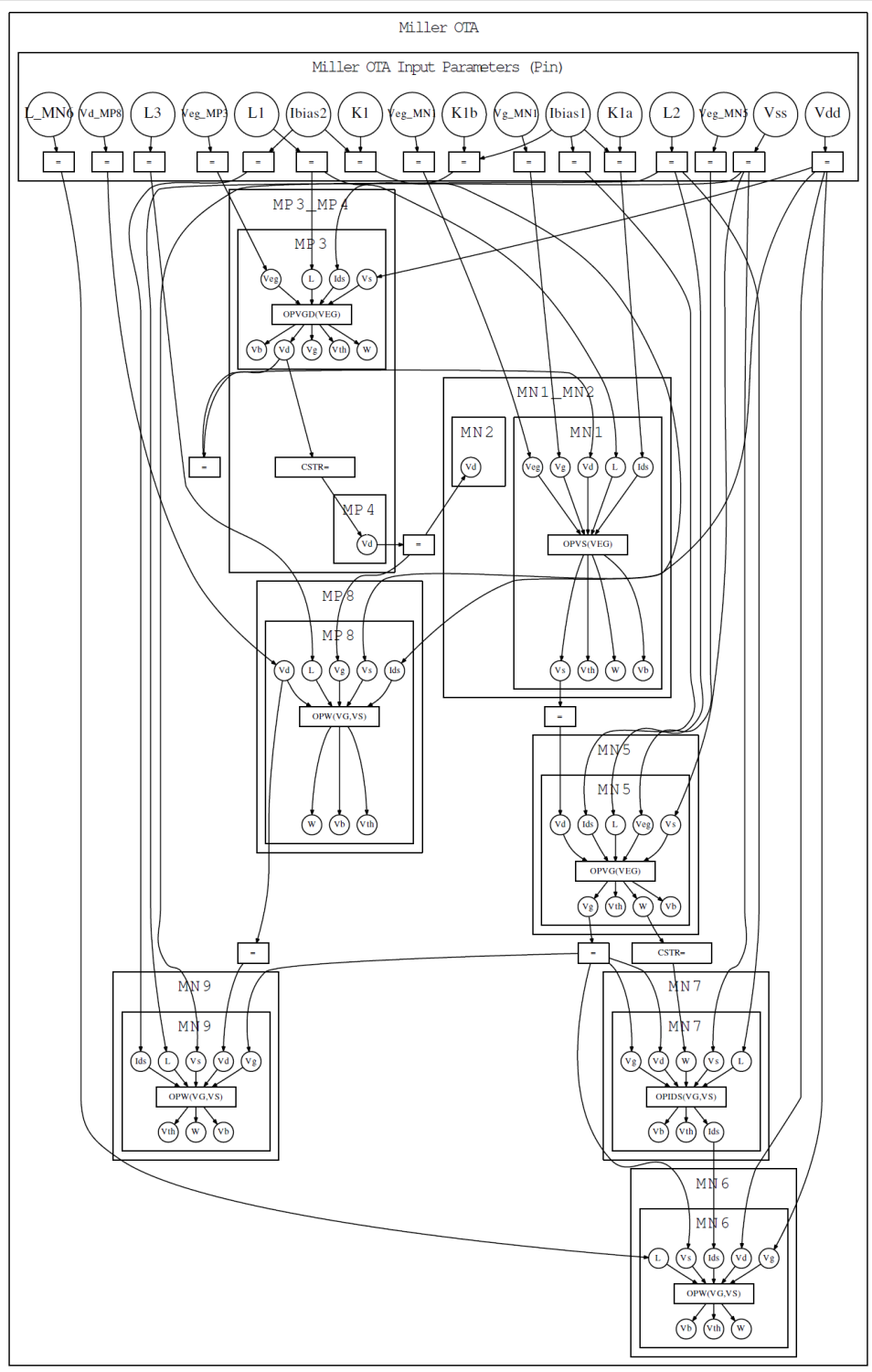
Figure 8: P-type computational model describing the DC design space of the Miller OTA amplifier
The complexity of this knowledge bipartite graph is linear with respect to the number of devices or nodes in the circuit. Therefore, it represents the P-type computational model for the OTA Miller describing the full design space of the DC operating point. It has been generated cognitively and without any data-driven learning.
We conclude that the analog circuit sizing optimization task is neither NP-Complete nor NP-Hard. It is solvable as a P-type problem.
What does it mean in terms of Computational Complexity ?
To answer this question, I used the reference [35] that describes the different theories of Time and Space complexities, as well as different definitions for P and NP and suggesting in page 69 and section 2.7 that most of the believes are suggesting that P ≠ NP.
Let us analyse the results mentioned above based on the contents of this book:
Since the task of synthesis was resolved using knowledge graph generation, we conclude that the set of designs Rdesign has design inputs x producing an output y using graph G(x,y):
Rdesign = { (x,y) : G(x,y) ≠ ∅ } and that Rdesign ∈ PF where PF is Polynomial Find set or Polynomial solvable set.
Similarly, the task of simulation of an arbitrary design (x,y) is defined as Rsimulation = { (x,y) : V(x,y) = 1 } where V(x,y) is the verification procedure or the NP-witness.
In addition, Rsimulation ∈ PC where PC is Polynomial Check set or Polynomial Verifiable Set.
Since the design (x,y) is arbitrary and that V(x,y) = 1 and there is always a graph G(x,y), we conclude that PC ⊆ PF.
Theorem 2.6 in page 63 states that if PC ⊆ PF, then P = NP.
Therefore, I claim that P= NP for x, y ∈ ℜ
Please do me a favor and CRITISIZE my findings.
References:
-
R.Harjani, R.A.Rutenbar, L.R.Carley, "OASYS: a framework for analog circuit synthesis," IEEE Transactions on Computer-Aided Design, vol. 8, no. 11, pp. 1247–1266, 1989.
-
M.G.R.DeGrauwe, E.D.O.Nys, J.Rijmenants, S.Bitz, B.L.A.G.Goffart, E.A.Vittoz, S.Cserveny, C.Meixenberger, G.vanderStappen, H.J.Oguey, "IDAC: an interactive designtool for analog CMOS circuits," IEEE Journal of Solid-State Circuits, vol. 22, no. 6, pp. 1106–1116, 1987.
-
H.Y.Koh, C.H.Sequin, P.R.Gray, "OPASYN: a compiler for CMOS operational amplifiers," IEEE Transactions on Computer-Aided Design, vol. 9, no. 2, pp. 113–125, 1990.
-
W.Nye, D.Riley, A.Sangiovanni-Vincentelli, A.L.Tits, "DELIGHT.SPICE: an optimization-based system for design of integrated circuits," IEEE Transactions on Computer-Aided Design, vol. 7, no. 4, pp. 501–518, 1988.
-
E.S.Ochotta, R.A.Rutenbar, L.R.Carley, "Synthesis of high-performance analog circuits in ASTRX/OBLX," IEEE Transactions on Computer-Aided Design, vol. 15, no. 3, pp. 273–294, 1996.
-
G.V.derPlas, G.Debyser, F.Leyn, K.Lampaert, J.Vandenbussche, G.Gielen, W.Sansen, P.Veselinovic, D.Leenaerts, "AMGIE: a synthesis environment for CMOS analog integrated circuits," IEEE Transactions on Circuits and Systems, vol. 20, no. 6, pp. 1037–1058, 2001.
-
M.Krasnicki, R.Phelps, R.A.Rutenbar, L.R.Carley, "MAELSTROM: efficient simulation-based synthesis for custom analog cells," in Proceedings of the Design Automation Conference, 1999, pp. 945–950.
-
R.Phelps, M.Krasnicki, R.A.Rutenbar, L.R.Carley, J.R.Hellums, "ANACONDA: robust synthesis of analog circuits via stochastic pattern search," IEEE Transactions on Computer-Aided Design, vol. 19, no. 5, pp. 567–570, 2000.
-
M.J.Krasnicki, R.Phelps, J.R.Hellums, M.McClung, R.A.Rutenbar, L.R.Carley, "ASF: a practical simulation-based methodology for the synthesis of custom analog circuits," in Proceedings of the IEEE International Conference on Computer-Aided Design, 2001, pp. 350–357.
-
A.Doboli, R.Vemuri, "Exploration-based high-level synthesis of linear analogue systems operating at low/medium frequencies," IEEE Transactions on Computer-Aided Design, vol. 22, no. 11, pp. 1556–1568, 2003.
-
R.A.Rutenbar, G.Gielen, "Hierarchical Modeling, Optimization and Synthesis for System-Level Analog and RF Designs," vol. 95, IEEE Press, 2007, pp. 1556–1568.
-
G.Stehr, M.Pronath, F.Schenkel, H.Graeb, K.Antreich, "Initial sizing of analog integrated circuits by centering with implicit topology given specification," in Proceedings of the IEEE International Conference on Computer-Aided Design, 2003, pp. 241–246.
-
D.Stefanovic, M.Kayal, P.A.D: a new interactive knowledge-based analog design approach," Analog Integrated Circuits and Signal Processing, vol. 45, pp. 291–299, 2005.
-
D.Stefanovic, M.Kayal, "Structured Analog CMOS Design," Kluwer Academic Publishers, 2009 (ISBN 978-1-4020-8572-7).
-
D.M.Binkley, C.E.Hopper, S.D.Tucker, B.C.Moss, J.M.Rochelle, D.P.Foty, "ACAD methodology for optimizing transistor current and sizing in analog CMOS design," IEEE Transactions on Computer-Aided Design, vol. 22, no. 2, pp. 225–237, 2003.
-
D.Binkley, "Tradeoffs and Optimization in Analog CMOS Design," John Wiley and Sons Inc., 2008 (ISBN 978-0-470-03136-0).
-
T.Morie, H.Onodera, K.Tamaru, "A method for analog circuit design that stores and reuses design procedures," Electronics and Communications in Japan, vol. 77, no. 1, pp. 87–96, 1994.
-
G.Gielen, P.Wambacq, W.Sansen, "Symbolic analysis for analog circuits: a tutorial overview," Proceedings of the IEEE, vol. 82, no. 2, pp. 287–304, 1994.
-
G.Gielen, W.Sansen, "Symbolic Analysis for Automated Design of Analog Integrated Circuits," Kluwer Academic Publishers, 1991 (ISBN 0792391616).
-
F.Fernandez, A.Rodriguez-Vazquez, J.L.Huertas, G.Gielen, "Symbolic Analysis Techniques: Applications to Analog Design Automation," IEEE Press, 1997 (ISBN-13 978-0780310759).
-
F.D.Bernardinis, M.Jordan, A.Sangiovanni-Vincentelli, "Support vector machines for analog circuit performance representation," in Proceedings of the Design Automation Conference, 2003, pp. 964–969.
-
Cochran & Cox, "Experimental Designs," John Wiley and Sons Inc., 1992, ISBN 0-471-54567-8.
-
F.Silveira, D.Flandre, P.G.A.Jespers, "A gm/ID based methodology for the design of CMOS analog circuits and its application to the synthesis of a silicon-on-insulator micropower OTA," IEEE Journal of Solid-State Circuits, vol. 31, no. 9, pp. 1314–1319, 1996.
-
P.Jespers, "The gm/ID methodology," in "A Sizing Tool for Low-Voltage Analog CMOS Circuits," Kluwer Academic Publishers, 2010 (ISBN 978-0-387-47100-6).
-
C.Enz, F.Krummenacher, E.Vittoz, "An analytical MOS transistor model valid in all regions of operation and dedicated to low-voltage and low-current applications," Analog Integrated Circuits and Signal Processing, vol. 8, pp. 83–114, 1995.
-
C.C.Enz, E.A.Vittoz, "Charge-Based MOS Transistor Modeling: The EKV Model for Low-Power and RF IC Design," John Wiley and Sons Inc., 2006 (ISBN 978-0-470-85541-6).
-
M.C.Schneider, C.Galup-Montoro, "CMOS Analog Design Using All-Region MOSFET Modeling," Cambridge University Press, 2010 (ISBN 9780521110365).
-
J.Vlach, K.Singhal, "Computer Methods for Circuit Analysis and Design," Kluwer Academic Publishers, 1983 (ISBN 0-442-28108-0).
-
H.Graeb, S.Zizala, J.Eckmueller, K.Antreich, "The sizing rules method for analog integrated circuit design," in Proceedings of the IEEE International Conference on Computer-Aided Design, 2001, pp. 343–349.
-
H.E.Graeb, "Analog Design Centering and Sizing," Kluwer Academic Publishers, 2007 (ISBN 978-1-4020-6003-8).
-
R.Phelps, M.J.Krasnicki, R.A.Rutenbar, L.R.Carley,J.R.Hellums, A case study of synthesis for industrial-scale analog IP: redesign of the equalizer/filter frontend for an ADSL CODE, in Proceedings of the IEEE 37th Design Automation Conference, DAC'00, June 2000, Pages 1–6.
-
A.Malak, Y. Li, R. Iskander, F. Durbin, F. Javid, M. M. Louërat, A. Tissot, J. M. Guebhard : “Fast multidimensional optimization of analog circuits initiated by monodimensional global Peano explorations”, Integration, the VLSI Journal, vol. 48, pp. 198-212, (Elsevier) (2015).
-
R. Iskander, M. M. Louërat, A. Kaiser : “Hierarchical sizing and biasing of analog firm intellectual properties”, Integration, the VLSI Journal, vol. 46 (2), pp. 172-188, (Elsevier) (2013).
-
R. Iskander, M. M. Louërat, A. Kaiser : “Automatic DC operating point computation and design plan generation for analog IPs”, Analog Integrated Circuits and Signal Processing, vol. 56 (1-2), pp. 93-105, (Springer Verlag) (2008).
-
Oded Goldreich: P, NP and NP-Completeness: The Basics of Computational Complexities, Cambridge University Press, 2010.
